THE OPU
The constraints
are now physical.
AI demand growth has outstripped the growth of the systems that support it.
Neurophos
Solves Both
How much
can you manufacture?
Every expansion plan hits the same constraint: compute per wafer.
More compute
per fab.
Fabs process a fixed number of wafers per day. Today, each wafer produces a certain amount of compute. The OPU breaks that constraint.
By compressing rack-level performance into a single package, each wafer delivers 50× the compute, on conventional production lines.
The OPU upgrades every fab into a hyperfab.
How much
can you power?
Demand keeps scaling with larger models, longer prompts, and agentic workloads. Power infrastructure is not scaling that fast.
More compute
per gigawatt.
Power is becoming the binding constraint on AI deployment. The OPU breaks that constraint.
It delivers 30× more performance per watt on real inference workloads, compressing what would traditionally require a GPU rack into the power envelope of a single package.
TW compute at GW scale.
“Moore's Law has slowed, but AI can't afford to wait.
Our breakthrough in photonics unlocks an entirely new dimension of scaling — by packing massive optical parallelism on a single chip.”
0×
SMALLER
The Questions You're
Actually Asking.
Decode is memory-bandwidth limited, not compute-limited. The industry is making strong progress there. We focus on prefill — the compute-bound bottleneck that represents 93% of inference tokens.
Photonic tensor cores operate natively at low-bit precision operands (INT4/FP4) — the same precisions used by modern inference workloads — and perform summation with effectively full precision accumulators.
Yes. Manufactured on standard CMOS. No exotic materials. No custom fabs.
Multi-chip module with electronic companion die for memory and I/O. Standard server rack integration — no rewrites to the surrounding stack.
Optical cores consume energy only for I/O — matrix multiplication becomes nearly free in the photonic domain. Efficiency improves quadratically with array size.
Tulkas T100 ships in 2028. Production capacity is allocated ahead of delivery — contact us to discuss timelines.
Help build
the OPU.
We're hiring across photonics, analog, digital, packaging, and software in Austin and Sunnyvale.
10,000×
SMALLER.
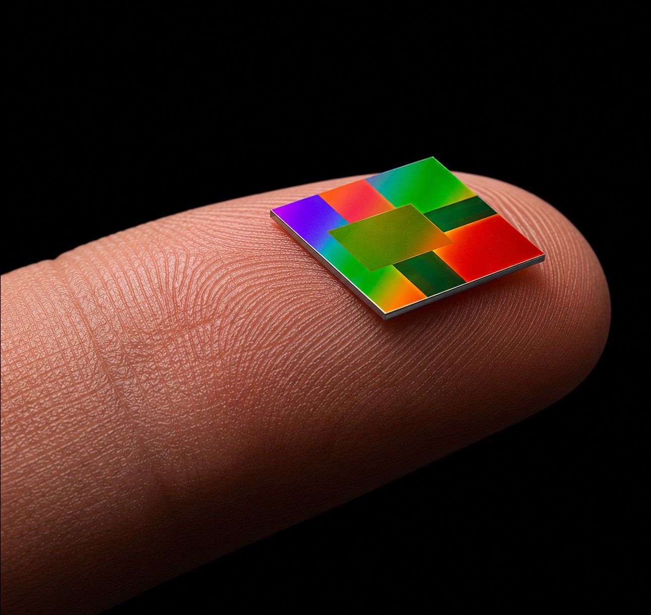
1 million photonic elements fit in 3% of a reticle chip the size of a postage stamp. What used to fill a meter-squared optical bench now rides on the tip of a finger — on conventional CMOS lines, no exotic materials, no bespoke fabs.
≈ 33 million elements would fit in a single postage-stamp die.
Each wafer that leaves the fab now carries the compute formerly spread across a server rack. The economic unit of AI shifts from the rack to the die.
THE POWER
ENVELOPE.
Optical cores consume energy only for I/O. Matrix multiplication, once the dominant cost of inference, becomes nearly free in the photonic domain. Efficiency improves quadratically with array size.
THE
BREAKTHROUGH.
A new class of optical compute fabric that performs matrix multiplication in the photonic domain. Compact, CMOS-compatible, and scaled on standard silicon — unlocking efficiency and density previously thought decades away.
Built on standard CMOS processes. No exotic materials. No bespoke fabs. Every wafer that leaves the line carries rack-scale compute on a 25 mm² die.
CONTACT.
Reach the team directly — product inquiries, technical deep-dives, and partnership conversations are all welcome.
BUILD
WITH US.
We're assembling a small, deeply technical team across photonic device engineering, ASIC design, compilers, and systems. If the physics of the problem excites you, we want to hear from you.
Don't see your role? Write to careers@neurophos.com with what you'd build here.